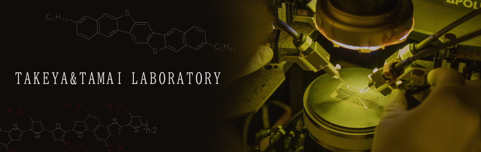
In the development of next-generation electronic devices, it is needed to consider their compatibility to the environment and demands for their diverse functions because of the rapid structural change in human society. Recently, organic semiconductor devices are attracting much attention as a practical candidate to meet such requirements because of their simple and low-cost production processes, low environmental burden, as well as for their unique function of flexibility. The scope of our research group ranges from basic scientific studies on materials chemistry and charge transport physics in organic semiconductor interfaces to the device functionalization and engineering of organic semiconductors.
Research Programs
- Development of high-performance organic devices and their matrix arrays
- Synthetic chemistry to develop high-performance organic semiconductors
- Fundamental charge transport mechanisms in high-mobility organic semiconductors
- Interfaces of organic hetero-junctions: development and functions of their two-dimensional electronic states
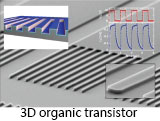
1. Development of high-performance organic devices and their matrix arrays
Development of world’s best-performing printable organic transistors
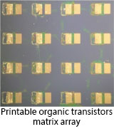 Organic semiconductors have unique features that they can be fabricated by simple “printing” processes from their solution, causing pronounced impact in the discussion on novel low-cost electronic devices with low environmental burdens as compared to the existing semiconductor industry using inorganic materials. We are leading the development of high-performance printable organic semiconductors with the development of solution-crystallization processes. Achieving the mobility of exceeding 10 cm2/Vs, this method has enabled more than one-order higher-speed charge motion than in previous solution-processed organic devices, so that further advanced technologies for high-performance semiconductor arrays are under development to provide practical circuitry and display matirices.
Active matrices and high-speed circuitries
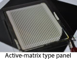 Our organic transistors already outperform the conventional counterpart of amorphous silicon TFTs by more than one-order higher mobility. Using the printed low-cost and large-area arrays of the transistors with the mobility of 10 cm2/Vs, we start developing high-speed circuitries and active-matrix displays. The achievement accelerates industrialization of flexible displays, electronic papers, various sensor panels, and RFID tags.