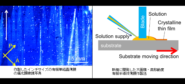
インチサイズの有機半導体単結晶薄膜
今まで有機半導体には、軽くて大面積に印刷可能、かつ低コストという長所が認められてきました。ディスプレイやRF-IDタグなどの高速でon/offを切り替える必要のある部材に応用する場合、高いキャリア伝導性能が必要とされていますが、これまでの一般的な手法でデバイスを作製した場合、キャリア伝導性能を作製プロセスでロスしてしまうという課題がありました。
これは、従来のスピンコート法などの作製方法ではミクロン級の微小な結晶しかできず、ゆえにキャリア伝導性能が低いことに依ります。
そこで、有機半導体を用いるメリットである低コストで大面積デバイスを作製可能という長所を犠牲にすることなく、高いキャリア伝導性能を持ち、かつ容易に有機半導体薄膜を作製可能な方法を開発することが課題となっていました。
竹谷研究室では、2009年11月に発表した塗布結晶化法の改良を進め、このたびインチサイズの大面積に単結晶薄膜を結晶化できるようになりました。
これにより、今まで実現困難だった、高速・大面積ディスプレイの駆動回路作製が容易に実現可能となりました。今後、RF-IDタグ等の高速アプリケーションへの応用が期待されます。
本成果は Applied Physics Express オンライン版に掲載されました。
- Inch-Size Solution-Processed Single-Crystalline Films of High-Mobility Organic Semiconductors
J. Soeda, T. Uemura, T. Okamoto, C. Mitsui, M. Yamagishi, and J. Takeya
Appl. Phys. Exp. 6, 076503 (2013)
DOI: 10.7567/APEX.6.076503Abstract:
A method for continuously growing large-domain organic semiconductor crystals is developed to fabricate multi-array high-mobility organic transistors. An organic semiconductor solution is held at the edge of a moving blade to grow a large-area crystalline thin film. The continuous evaporation of the solvent at around 100 °C, while the solution is supplied at the same rate, allows the organic crystals to grow steadily on the substrate to several inches in size. The performance of the arrays of field-effect transistors based on the large-domain crystal films is excellent, with mobility of 5–10 cm2 V-1 s-1.